The manufacturing of semiconductor silicon wafers involves high-precision processes where nanometer-scale features must be kept clean from foreign particles, organic outgassing, and electrostatic discharge. As fabrication facilities advance to sub-7nm process nodes, the requirements for contamination control during storage and transport have intensified. A specialized wafer containers factory serves as a fundamental link in the supply chain, engineering protective packaging to prevent yield loss. This analysis examines the engineering processes, material requirements, and cleanliness protocols employed within a production facility to ensure that silicon wafers remain secure between processing stages.
To protect fragile silicon substrates, a Hiner-pack production line utilizes specialized engineering polymers. The choice of polymer determines the carrier’s thermal stability, structural stiffness, and chemical resistance. Standard plastics can degrade or release volatile components under cleanroom conditions, making precise material selection necessary for wafer safety.
Standard wafer carriers often employ Polycarbonate (PC) due to its dimensional stability, transparency, and impact resistance. However, for high-temperature applications or automated materials handling systems (AMHS), alternative materials are selected:
Polyetheretherketone (PEEK): Known for its thermal properties, chemical resistance, and minimal wear particle generation. It is often chosen for front-opening unified pods (FOUPs) operating in continuous-use environments.
Polybutylene Terephthalate (PBT): Offers mechanical strength and dimensional stability under varying humidity levels, preventing deformation that could disrupt automated robotic grippers.
Polypropylene (PP): Frequently applied in raw wafer shipping and storage due to its balance of flexibility and cost-efficiency, mitigating mechanical shocks during international transit.
Electrostatic charge accumulation poses two major challenges: electrostatic attraction (ESA) of airborne particles and electrostatic discharge (ESD) which can damage microcircuitry. A specialized wafer containers factory integrates carbon powder, carbon fibers, or inherently dissipative polymers into the raw material matrix during formulation. This creates a conductive or static-dissipative material with a surface resistivity typically ranging from 104 to 1011 ohms per square. This controlled conductivity allows static charges to bleed off safely, avoiding sudden electrostatic discharges that could destroy active components on the wafer surface.
Producing high-purity wafer shippers requires specialized production machinery. Hiner-pack utilizes precise injection molding machines inside controlled environments to minimize contamination during the plastic melt stage. Robotic demolding systems transfer the cooled carrier bodies directly to assembly lines without human contact, avoiding contamination from skin oils, fibers, or perspiration.
The manufacturing process relies on exact control over molding parameters to prevent structural defects that could shed particles during use:
Mold Design and Tooling: High-precision steel molds are engineered with mirror-polished finishes. This prevents micro-flashes or burrs along the wafer slots, which could scrape the wafer edges and generate silicon dust.
Parameter Monitoring: Injection molding machines monitor melt temperature, injection pressure, and holding time in real time. Consistent wall thickness is necessary to prevent warping, which could cause wafer misalignment in automated processing tools.
Hot Runner Systems: These systems minimize material degradation during the molding cycle, ensuring that the physical and chemical properties of the polymer remain uniform throughout the entire container body.
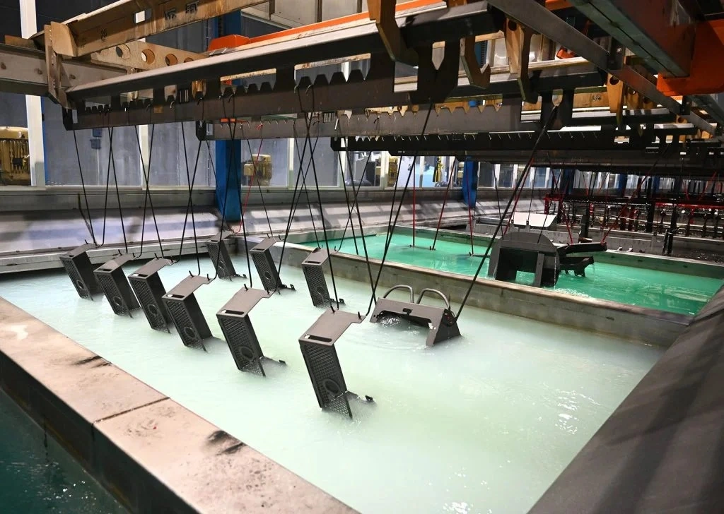
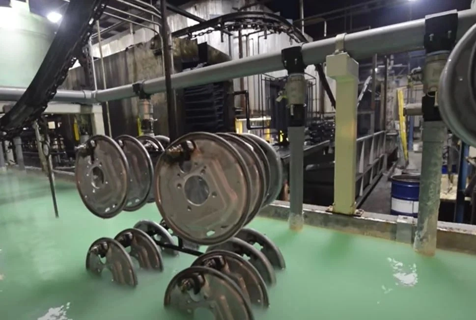
Once molded, wafer carriers undergo extensive post-processing to remove any residual surface contaminants before they are packaged and shipped to semiconductor fabrication plants:
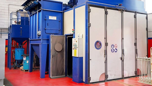
Air Filtration: Assembly, washing, and sealing take place within ISO Class 4 (Class 10) or ISO Class 5 (Class 100) cleanrooms. High-Efficiency Particulate Air (HEPA) and Ultra-Low Penetration Air (ULPA) filtration units cycle the air constantly, maintaining strict particle count thresholds.
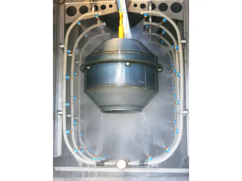
Ultrapure Water (UPW) Washing: Carriers undergo automated washing cycles utilizing UPW with resistivity levels reaching 18.2 Megohm-cm. This process rinses away residual mold-release agents, organic micro-contaminants, and surface ions.
Deionized Nitrogen Drying: After washing, carriers are dried using heated, ultra-pure nitrogen gas to eliminate water spots and prevent any localized oxidation on metal structural components like hinges or latches.
Vacuum Packaging: Finished products are sealed inside multi-layer, static-shielding barrier bags under cleanroom conditions. This prevents the ingress of environmental particulates and moisture during global logistics.
Transporting wafers between fabrication facilities, metrology labs, and packaging houses involves physical challenges, including mechanical vibrations and potential drops. A specialized wafer containers factory designs structures tailored to mitigate these physical impacts.
Different transport scenarios require different container designs to optimize protection and space:
Coin Style Shippers (Single Wafer Shippers): Designed for shipping individual, high-value wafers or thin substrates. These containers secure the wafer between soft, low-outgassing elastomer cushions. The screw-top or snap-on lid design prevents pressure build-up while keeping the silicon substrate centered.
Horizontal Wafer Shippers (Multi-Wafer): For shipping batches of 25 wafers, horizontal shippers utilize a high-density polyethylene (HDPE) or polycarbonate housing equipped with a secure latch mechanism. Internal spring retainers apply gentle downward force on the edges of the wafers, preventing movement along the X, Y, or Z axes during transit.
Modern semiconductor fabrication facilities rely on automated systems to move wafers between processing tools. The containers must be designed to interface with these systems:
Front-Opening Unified Pods (FOUPs): Facilitate automatic loading and unloading by matching exact robotic interface dimensions defined by SEMI standards. The front door must seal tightly to maintain an isolated nitrogen or dry air environment inside.
Front-Opening Shipping Boxes (FOSBs): Provide robust external protection for long-distance transit. They are designed to load onto automated sorters and metrology equipment, allowing automated systems to unpack wafers without manual intervention.
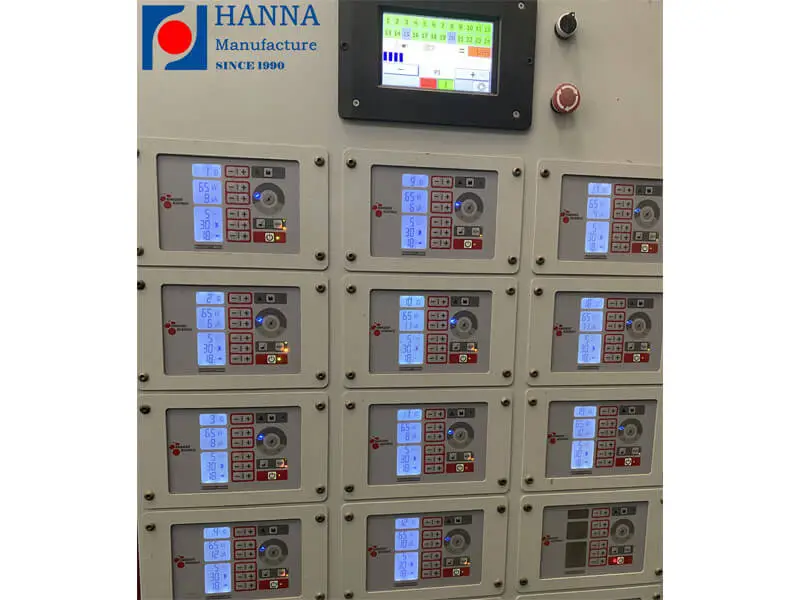
At Hiner-pack, quality assurance goes beyond visual inspections to implement scientific verification methods. The performance of a wafer container must be verified through objective testing before it enters cleanroom operations.
To confirm that the wafer containers do not introduce contaminants, manufacturers perform regular laboratory testing on production samples:
Liquid Particle Counter (LPC) Tests: This test involves submersing sample carriers in high-purity water and applying ultrasonic energy to dislodge surface particles. The water is then analyzed to count and size the dislodged particles, ensuring they remain below strict allowable limits.
Gas Chromatography-Mass Spectrometry (GC-MS): Testing the outgassing potential of polymers to ensure that volatile organic compounds (VOCs) do not deposit on active wafer surfaces during storage, which could cause chemical contamination.
Ionic Contamination Testing: Measuring trace levels of elements like sodium, iron, or copper on the carrier surface, as these ions can diffuse into the silicon lattice and alter electrical characteristics.
A wafer container must maintain precise dimensions to prevent automation jams and mechanical damage to wafers:
Coordinate Measuring Machines (CMM): These machines verify that wafer spacing, latch alignment, and robotic interface pins match SEMI guidelines to within microns.
Deformation Resilience under Load: Testing long-term structural integrity when stacked in warehouse racking or transported on high-speed conveyor lines. The container must resist sagging or warping under load to maintain automated compatibility.
The progression toward 2.5D/3D integration, chiplets, and wafer-level packaging requires custom wafer handling configurations. Thin wafers, reconstituted wafers, and wafers with high solder bumps present unique structural challenges. A qualified wafer containers factory works with process engineers to modify interior pocket designs, integrate custom cushioning materials, and develop custom slot pitches to accommodate thick or bowed wafers without contact with the active wafer surface.
Q1: Why is ESD protection vital for wafer carriers during
shipping?
A1: ESD protection is vital because
static charges attract airborne micro-particulates to the wafer surface and can
cause high-voltage discharge that destroys microscopic circuit patterns.
Integrating static-dissipative additives into carrier polymers mitigates these
issues.
Q2: What is the difference between FOUP and FOSB
containers?
A2: A FOUP (Front-Opening Unified Pod)
is designed for internal fab transport and automation tool docking in cleanroom
environments. A FOSB (Front-Opening Shipping Box) is structured for
inter-facility transport, providing enhanced protection during long-distance
shipping.
Q3: How does outgassing from wafer packaging affect semiconductor
yields?
A3: Outgassing occurs when volatile
compounds evaporate from the packaging plastic and deposit on the silicon
surface. These trace organic contaminants can block chemical reactions during
deposition or etching steps, leading to device malfunction and yield loss.
Q4: What SEMI standards apply to wafer
containers?
A4: SEMI standards, such as SEMI E1.9,
E47.1, and E110, define the mechanical interfaces, dimensions, and automated
handling specifications for wafer carriers to ensure compatibility with
processing tools globally.
Q5: How are wafer shippers cleaned before
reuse?
A5: Reusable wafer shippers undergo
multi-stage automated washing processes utilizing hot ultrapure water (UPW),
mild surfactant solutions, and high-purity nitrogen drying to remove accumulated
particles and chemical contaminants.
For semiconductor packaging plants and raw wafer manufacturers, choosing reliable containment is necessary to secure yield throughout the distribution chain. Our engineering team provides custom and standard solutions to address complex cleanroom storage and transport requirements. Please contact us to request product specifications, sample test reports, or to coordinate an engineering consultation for your specific process node requirements. Submit your Inquiry through our contact form, and our representatives will assist with your operational needs.